全国咨询热线
全国咨询热线

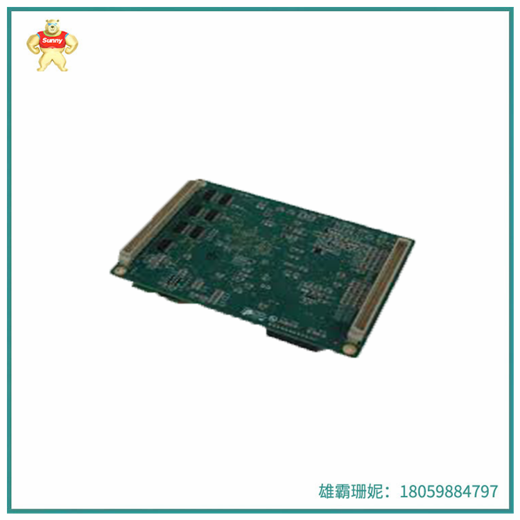
产品名称 :半导体基板
产品型号:810-800060-004
品牌:LAM
810-800060-004半导体基板是用于生长和制作半导体器件的基础材料,通常由硅、碳化硅、氮化铝、锗等材料制成。这些材料具有良好的电学和物理性能,是半导体器件制造的常用材料。根据材料的不同,半导体基板可分为硅基、碳化硅基、氮化铝基和锗基等多种类型。其中,硅基是目前应用广泛的基板类型,而碳化硅基和氮化铝基则主要应用于高功率和高频率器件制造,锗基则应用于红外、光电等领域。
810-800060-004半导体基板的制造工艺主要包括晶体生长、切片和抛光等步骤。晶体生长是指将基础材料生长成大尺寸的单晶片,常用的生长方法包括Czochralski法和Float-Zone法等。切片是将生长好的单晶片切割成小的晶片,以便后续的工艺加工。抛光则是为了去除晶片表面的缺陷,以提高器件性能。
810-800060-004半导体基板的质量和性能对半导体芯片和电子器件的效果有着至关重要的影响。因此,在半导体制造过程中,基板的选择和制造工艺的控制都至关重要。
Product name: Semiconductor substrate
Product model: 810-800060-004
Brand :LAM
810-800060-004 Semiconductor substrate is the base material for growing and making semiconductor devices, usually made of silicon, silicon carbide, aluminum nitride, germanium and other materials. These materials have good electrical and physical properties and are commonly used in semiconductor device manufacturing. According to the different materials, semiconductor substrates can be divided into silicon, silicon carbide, aluminum nitride and germanium and other types. Among them, silicon base is currently widely used substrate type, while silicon carbide base and aluminum nitride base are mainly used in high power and high frequency device manufacturing, germanium base is used in infrared, photoelectric and other fields.
810-800060-004 Semiconductor substrate manufacturing process mainly includes crystal growth, slicing and polishing steps. Crystal growth refers to the growth of the base material into a large size single wafer, and the common growth methods include Czochralski method and Float-Zone method. Slicing is the cutting of the grown single wafer into small wafers for subsequent processing. Polishing is to remove defects on the wafer surface to improve device performance.
810-800060-004 The quality and performance of the semiconductor substrate have a crucial impact on the effect of semiconductor chips and electronic devices. Therefore, in the semiconductor manufacturing process, the selection of the substrate and the control of the manufacturing process are crucial.
| 其他型号推荐 | ||
| LAM 685-069171-100 | LAM 853-059895-033 | LAM 853-064887-402 |
| LAM 853-800749-014 | LAM 714802323003B | LAM 853-039372-001 |
| LAM X9-3P3P3P2L-12 | LAM 853-042958-228 | LAM 853-801876-015 |
| LAM 853-801876-014 | LAM E204460 | LAM 853-300087-404 |
| LAM 853-801876-004 | LAM ASSY 1900001963-0000 | LAM 855-800256-107 |
| LAM 1034982-5113-2280 | LAM 685-069171-200 | LAM 605-064676-006 |
| LAM 714-801590-002/A | LAM 853-028873-497 | LAM 605-707109-012 |
| LAM 810-800060-004 | LAM 810-063892-001 | LAM 810-801237-021 |
| LAM BPC-1703 | LAM 61-465138-00 | LAM 853-800838-011 |
| LAM 676-067735-502 | LAM 853-800087-406 | LAM 715-031733-003 |
| LAM 810-800256-107 | LAM 853-069793-005 | LAM 713-031263-005 |
雄霸工控

微信二维码
Copyright © 2022-2024 厦门雄霸电子商务有限公司 版权所有 备案号:闽ICP备14012685号-33